
Capability 01 — Design & Engineering
Key feel, radio range and firmware are one design problem.
A remote has no screen to explain itself. The housing, the key geometry and the firmware timing all contribute to whether it feels responsive or cheap — which means they cannot be designed in isolation.
The brief
Three problems are solved by the same millimetre.
The gap that gives a key its travel also changes how much dust can enter. The battery tube changes where the antenna can sit. The tooling draft changes how the seam reads in the hand.
We resolve those conflicts in CAD and on a breadboard before tooling, because changing a mold is the most expensive way to learn about them.
- A key map that can be explained in one sentence per group
- RF performance measured through the final housing
- Battery budget consistent with the stated use pattern
- A housing that can be assembled and tested repeatably
- Documentation that survives a supplier change
Disciplines
Five workstreams, reviewed together.
Design reviews include all five so a decision in one does not silently break another.
Form that explains itself
Silhouette, balance and CMF. Key grouping is treated as information design: primary keys get size and position, secondary keys get distance.
Structure and assembly
Wall thickness, draft, snap fits, sealing and battery access. We design for the assembly fixture and the test fixture at the same time.
Board, antenna and power
Key matrix, IR driver, radio module placement and battery path. Antenna clearance is checked against the final enclosure materials, not the dev board.
Logic that can be tested
Scanning, debounce, repeat behavior, protocol stack and update path. Each behavior has a test case the QA team can run on production units.
Designed for the line
Component availability, panelization, test points and assembly time are reviewed before tooling release. A design that cannot be built at volume is not finished.
A package someone can inherit
Approved drawings, BOM, firmware release notes and test specifications. The program should not depend on one engineer’s memory.
The team
Thirty-two engineers, two named owners.
The electronic and software chain is led by our R&D director, who has spent more than twenty years in the remote industry. The hardware and tooling chain is led by a mechanical engineer with more than twenty-five years in tooling. Both sit in the same review, so a PCB decision meets the mold decision before either is released.
From SoC selection to factory test software
- BLE SoC selection: Realtek, Telink, OnMicro
- RFQ evaluation and PCB layout
- PCBA build and firmware design
- App (APK) design
- Factory test software and PCBA test modes
From customer ID to mass production
- Customer ID evaluation and 3D review
- DFM report and tooling design review
- T0 / T1–Tn sample review with issue lists
- Golden sample sign-off and pilot build
- First mass production and quality control
Tooling economics
A common mold base, 5–8% cheaper every year.
A shared mold base shortens tooling design and lets a second variant reuse an existing frame. On programs that adopt it, the company target is a 5–8% reduction in tooling cost each year for three years.
Reduction target for three years on common-base programs.
Measured across successive variants, not a one-off quote.
Target risk at the mechanical, tooling and injection check points.
From ID evaluation to first mass production, each step with a report.
| Engineer | Checks | Effect |
|---|---|---|
| Mechanical | 3D design and housing fit | Design risk held under 5% |
| Tooling | Tooling design and housing parts | Tooling risk held under 5% |
| Injection | Injection parameters and housing quality | Stable quality and a reasonable cycle |
Measured on delivered programs. Results on a new housing or volume are confirmed during validation.:
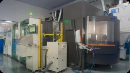
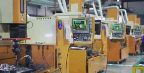
Design, tooling, first shots

Artifacts
What you review at each handoff.
Nothing moves to the next stage on a verbal approval. Each artifact has a revision and an owner.
| Stage | Artifact | What it decides |
|---|---|---|
| Concept | Key-map drawing and CMF direction | Hierarchy, legends, material and finish |
| Design freeze | 3D assembly, 2D drawings, BOM | Tooling, tolerances, component choices |
| Prototype | Functional sample and firmware build | Key feel, RF range, power draw, behavior |
| Validation | Test plan and result report | Reliability, pre-scan, protocol conformance |
| Production release | Test specification and fixture list | What every unit is checked against |
Working with your team
We can lead the design or fit into yours.
Some clients have an ID partner and need manufacturing engineering. Others have firmware and need the mechanical and radio work. The boundary is agreed at the brief stage.
When your team owns a workstream, we ask for the same artifacts we would produce — drawings, BOM, release notes — so the integration is not based on assumptions.
Questions
Design & engineering FAQ
Can you work from our existing 3D files?
Who owns the design files?
How do you verify key feel without a production mold?
Do you design the retail packaging?
Start a project
Send the files you have. We will list the gaps.
ID renders, a competitor sample, a receiver and a launch date are enough to start a useful conversation.